

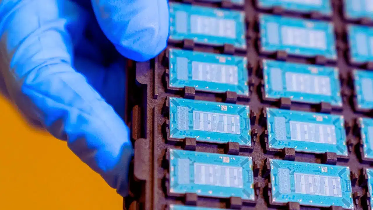
Intel says it is pushing High-NA EUV toward production by completing key tool milestones in Oregon while ramping Intel 18A toward high-volume manufacturing in Arizona, aiming to extend chip scaling beyond today’s EUV era.
What Intel said and did
Intel Foundry previously announced the completed assembly of what it described as the industry’s first commercial High Numerical Aperture (High-NA) EUV lithography scanner at its Hillsboro, Oregon R&D site, with the tool entering calibration for future process nodes.
Intel also disclosed a separate milestone: Intel and ASML reached “acceptance testing” on ASML’s TWINSCAN EXE:5200B High-NA EUV tool, which Intel said achieved 175 wafers per hour and 0.7 nanometer overlay accuracy (layer-to-layer alignment).
In parallel, Intel says its leading-edge Intel 18A process has entered “risk production,” described by the company as the final stage before volume production, with high-volume production expected in the second half of 2025.
Intel’s latest client roadmap also ties manufacturing readiness to products: the company says Panther Lake (its first AI PC platform built on Intel 18A) is intended to enter high-volume production at Intel’s Fab 52 in Chandler, Arizona later in 2025.
These updates together signal Intel’s near-term focus on scaling 18A while preparing High-NA EUV for the next major node transition to Intel 14A.
What High-NA EUV is
High-NA EUV is a next-generation version of EUV lithography that increases numerical aperture (NA)—a measure of how well an optical system can collect and focus light—to improve resolution and pattern smaller features on silicon.
Intel says High-NA EUV (0.55NA) can deliver higher imaging contrast than today’s commonly used 0.33NA EUV for similar features, potentially enabling less light per exposure and faster layer printing, which can raise wafer output.
Intel also describes High-NA EUV as an “evolutionary step” beyond EUV lithography, which uses 13.5 nm wavelength light created by firing a powerful laser at tiny tin droplets to generate EUV light.
ASML states that the first High-NA EUV lithography system was delivered in December 2023, marking the start of broader industry work to industrialize the platform.
Intel says its High-NA EUV tool was transported to Oregon in more than 250 crates inside 43 freight containers, with each system weighing more than 150 metric tons—underscoring the scale and complexity of deploying these tools.
Why this matters for 18A now and 14A next
Intel’s public roadmap links High-NA EUV to maintaining scaling momentum after Intel 18A, with Intel saying it expects to use both 0.33NA EUV and 0.55NA EUV in development and manufacturing “starting with product proof points on Intel 18A in 2025” and continuing into production of Intel 14A.
In practical terms, this positions 18A as the near-term node that must ramp reliably, while High-NA EUV becomes a key enabler for Intel 14A’s tighter patterning requirements.
Intel also says High-NA EUV, when combined with other process technology improvements, is expected to print features up to 1.7x smaller than existing EUV tools and enable up to 2.9x more density through 2D scaling.
From Intel’s perspective, the High-NA EUV toolchain is not a single switch, but a staged rollout: assembly and calibration of early tools, acceptance testing of more production-oriented systems, and then gradual integration into specific layers as process recipes mature.
The acceptance-testing milestone matters because it centers on manufacturing-grade metrics—throughput and overlay—that strongly influence yield, cycle time, and cost per chip.
Key specs and claims (from Intel and ASML statements)
| Item | What it refers to | Reported figure | Why it matters |
| Current mainstream EUV class | “Low-NA” EUV used broadly in leading-edge fabs | 0.33 NA | Baseline resolution and productivity for today’s EUV patterning. |
| High-NA EUV class | Next-gen EUV optics | 0.55 NA | Higher imaging contrast and improved resolution headroom. |
| Feature scaling expectation | High-NA vs existing EUV tools (Intel expectation) | Up to 1.7x smaller features | Can reduce reliance on multi-patterning and push density higher. |
| Density expectation | 2D scaling enabled by High-NA (Intel expectation) | Up to 2.9x more density | Supports more transistors per area for performance and efficiency gains. |
| Production tool milestone | EXE:5200B acceptance testing (Intel/ASML milestone) | 175 wafers/hour; 0.7 nm overlay | Throughput and alignment are core prerequisites for high-volume manufacturing. |
| Platform starting point | First High-NA EUV system delivery (ASML statement) | Delivered Dec 2023 | Signals platform availability moving from labs into customer sites. |
What comes next for the chip industry
Intel says it is building a “well-rounded lithography toolbox” and expects High-NA EUV to help drive process capabilities beyond Intel 18A into the second half of the decade.
At the same time, Intel is messaging execution on nearer milestones—especially the transition from 18A risk production into high-volume manufacturing in the second half of 2025—because successful ramp is essential before the industry will view High-NA EUV as more than an R&D headline.
Separately, Intel continues to expand EUV-based manufacturing capacity across regions, including prior announcements about high-volume production using EUV on Intel 4 in Ireland, reflecting how “standard” EUV has become foundational for advanced nodes.
In the near term, the most important indicators to watch will be: (1) confirmed 18A volume output for flagship products, (2) continued High-NA EUV tool qualification and stability, and (3) evidence that High-NA can reduce process complexity (fewer patterning steps) enough to justify its cost in production.
Final thoughts
Intel’s combined updates—18A moving through risk production toward high-volume output and High-NA EUV advancing through calibration and acceptance testing—show a two-track strategy: deliver on 2025 manufacturing commitments while preparing the lithography leap needed for 14A.
If Intel can sustain throughput, overlay, and yield targets as it scales 18A and integrates High-NA EUV into future layers, it could strengthen its position both as a CPU maker and as a contract foundry for external customers.